- 您现在的位置:买卖IC网 > Sheet目录344 > MSL1061AV (Atmel)IC LED DRIVER 6 STRING
Atmel LED Drivers-MSL1061/MSL1064
6-string PWM LED Driver with Digitally Compensated, 1.1MHz,
48V Boost Regulator, ±1.5% Current Balance, I 2 C Interface
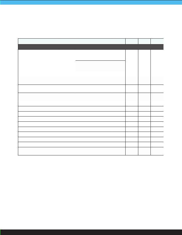
PARAMETER
SYMBOL
CONDITIONS AND NOTES
MIN
TYP
MAX
UNIT
I2C SWITCHING CHARACTERISTICS
SCL clock frequency
Bus time-out period
STOP to START condition bus
free time
Repeated START condition
hold time
Repeated START condition
set-up time
STOP condition set-up time
SDA data hold time
SDA data valid acknowledge time
SDA data valid time
SDA data set-up time
SCL clock low period
SCL clock high period
SDA, SCL fall time
SDA, SCL rise time
SDA, SCL input suppression
filter period
1/t SCL
t TIMEOUT
t BUF
t HD:STA
t SU:STA
t SU:STOP
t HD:DAT
t VD:ACK
t VD:DAT
t SU:DAT
t LOW
t HIGH
t F
t R
t SP
TOEN bit D1=0 in control
register to disable bus
timeout
TOEN bit D1=1 in control
register to enable bus
timeout
(Note 3)
(Note 4)
(Note 5, Note 6)
(Note 7, Note 10)
0
0.066
15
0.5
0.26
0.26
0.26
5
0.05
0.05
100
0.5
0.26
25
50
1000
0.55
0.55
120
120
kHz
ms
μs
μs
μs
μs
ns
μs
μs
ns
μs
μs
ns
ns
ns
Note 1. All parameters are tested at T A =25°C, unless otherwise noted. Specifications at temperature are guaranteed by design
Note 2. Minimum SCL clock frequency is limited by the bus timeout feature, which resets the serial bus interface if either SDA or SCL is held low for
t timeout . Disable the bus timeout feature for DC operation
Note 3. t VD:ACK = SCL LOW to SDA (out) low acknowledge time
Note 4. t VD:DAT = minimum SDA output data-valid time following SCL low transition
Note 5. A master device must internally provide an SDA hold time of at least 300ns to ensure an SCL low state
Note 6. The maximum SDA and SCL rise times is 300ns. The maximum SDA fall time is 250ns. This allows series protection resistors to be
connected between SDA and SCL inputs and the SDA/SCL bus lines without exceeding the maximum allowable rise time
Note 7. MSL1061/64 includes input filters on SDA, SCL, and AD0 inputs that suppress noise less than 50ns
Note 8. Subject to thermal dissipation characteristics of the device
Note 9. When mounted according to JEDEC JEP149 and JESD51-12 for a two-layer PCB, θ JA = 24.1°C/W, and θ JC = 2.7°C/W
Note 10. Guaranteed by design and characterization. Not production tested
Note 11. STR0 to STR5 current matching is the difference of any one string current and the average of all string currents divided by the average of
all string currents
Note 12. The MSL1061/64 selects the string (STR0 through STR5) with the lowest voltage to control the boost regulator voltage
Atmel LED Drivers-MSL1061/MSL1064
13
发布紧急采购,3分钟左右您将得到回复。
相关PDF资料
MSL2041GU
IC LED DRIVER 4 STRING
MSL2100BR
IC LED DRIVER 8 STRING
MSL2160DQ
IC LED DRIVER 16 STRING
MSL2162DQ
IC LED DRIVER 16 STRING
MSL3082CS
IC LED DRIVER 8 STRING
MSL3085BT
IC LED DRIVER 8 STRING
MSL3162BT
IC LED DRIVER 16 STRING
MSL3164BT
IC LED DRIVER 16 STRING
相关代理商/技术参数
MSL1061AV-R
功能描述:LED照明驱动器 6Str LED Dvr Dgtl 1.1MHz 48V r 1.5%
RoHS:否 制造商:STMicroelectronics 输入电压:11.5 V to 23 V 工作频率: 最大电源电流:1.7 mA 输出电流: 最大工作温度: 安装风格:SMD/SMT 封装 / 箱体:SO-16N
MSL1064
制造商:ATMEL 制造商全称:ATMEL Corporation 功能描述:6-string PWM LED Driver with Digitally Compensated, 1.1MHz, 48V Boost Regulator, ±1.5% Current Balance, I2C Interface
MSL1064AW
功能描述:LED照明驱动器 6Str PWM LED Dvr Dgt 1.1MHz 48V 1.5% I
RoHS:否 制造商:STMicroelectronics 输入电压:11.5 V to 23 V 工作频率: 最大电源电流:1.7 mA 输出电流: 最大工作温度: 安装风格:SMD/SMT 封装 / 箱体:SO-16N
MSL1064AW-R
功能描述:LED照明驱动器 6Str PWM LED Dvr Dgt 1.1MHz 48V1.5% I
RoHS:否 制造商:STMicroelectronics 输入电压:11.5 V to 23 V 工作频率: 最大电源电流:1.7 mA 输出电流: 最大工作温度: 安装风格:SMD/SMT 封装 / 箱体:SO-16N
MSL1064-TC
功能描述:LED照明驱动器 6Str PWM LED Dvr Dgt 1.1MHz 48V+/-1.5% I RoHS:否 制造商:STMicroelectronics 输入电压:11.5 V to 23 V 工作频率: 最大电源电流:1.7 mA 输出电流: 最大工作温度: 安装风格:SMD/SMT 封装 / 箱体:SO-16N
MSL106E
制造商:TE Connectivity 功能描述:
MSL-1-1/2
制造商:Cooper Bussmann 功能描述:
MSL-1-1/4
制造商:Cooper Bussmann 功能描述:
